Technology
Multilayer Printed Circuit Board: Definition, Benefits, and Manufacturing Process

If you are planning to build Multilayer Printed Circuit Boards for your next project, here is a guide to help you learn more about the boards.
In this article, you will learn what multilayer PCBs are, the advantages of using multilayer PCBs, why they are the most popular circuit boards, and the manufacturing process.
What is a multilayer PCB?
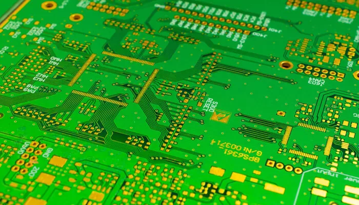
A multilayer PCB is a printed circuit board with three or more copper conductive layers. When you look at a multilayer PCB, the top and bottom layers look like a double-sided PCB. However, there are more layers on both sides. The layers are interconnected with copper-plated holes, where you can witness up to 40 layers.
Since multilayer PCBs can accommodate more components, they are widely used in various modern applications. Some applications include smart devices that need four to eight layers and smartphones that can use up to twelve layers.
When building a multilayer PCB, designers prefer even numbers over odd numbers. This is because laminating an odd number can be difficult and may lead to high costs. Happily, there is no limit to the number of layers that can be fabricated in a multilayer PCB.
Benefits of using multilayer PCB
Even though designing and making a multilayer PCB is a bit complex, it has several benefits. Here are the main advantages of a multilayer PCB.
1. Small size
Designs of multilayer PCBs use evolving manufacturing processes and rules to reduce the size of the boards. However, they still maintain the same functionalities. Hence, multilayer PCBs can be used in small, powerful gadgets such as smart devices requiring small-sized PCs.
2. Lightweight
Due to advancements in manufacturing techniques, multilayer PCBs have less weight than other types of circuit boards. The elimination of several connectors has led to the reduction of the weight.
3. High quality
A lot of work is done during manufacturing to produce high-quality multilayer PCBs. This makes them effective when used in smart devices such as smartphones. They possess many functionalities that single-layer PCBs or double-layer PCBs do not offer.
4. Durability and flexibility
Multilayer PCBs are built for long-term use. For instance, they are designed to withstand more weight, heat, and pressure. In addition, they are flexible to fit in according to the applications used.
5. Single connection point
Another benefit of using multilayer PCBs is that they are made to work on a single connection point. This is very crucial as it makes the boards effective. Hence, they are more functional than single-layer PCBs that need multiple connection points.
Design guideline for multilayer PCB
*Always have an even number of PCB layers. Even though it is possible to have an odd number, most manufacturers prefer an even number because it is cheaper.
*Make sure you pick the right PCB thickness and always think of the heavy components that will be added to the PCB board.
*Ensure you pick PCB slack based on design requirements. This is because the PCB engineer always chooses the ground method and power planes according to the circuit design.
*Always communicate with your manufacturer to understand their manufacturing capabilities.
Important Manufacturing Process
1. Oxide
Oxide is a manufacturing process that is only found when building multilayer PCBs. Oxide or Black Oxide is a chemical treatment for the inner layers of a multilayer PCB. It is used to increase clad copper’s roughness and enhance laminate bond strength.
In addition, the process helps to prevent delamination or separation of layers once the manufacturing process is complete.
2. Lamination
When building multilayer PCBs, alternating layers of epoxy-infused fiberglass sheet known as prepreg and the conductive core materials are laminated together. This is done under high pressure and temperature using a hydraulic press.
The high pressure and heat make the prepreg melt and manage to join the layers together. Once it cools down, it undergoes manufacturing steps as a double-layer PCB.
3. Drilling
Printed Circuit Boards typically require several drilled holes to attach components, link copper layers together, and mount the PCB in its housing. The holes are drilled using advanced drilling systems.
Drilling is done through a stack of two to three panels at a time, based on the volume being handled. The hole locations and sizes are programmed to the drill machine according to the data submitted by the designer.
4. Surface finish
The final chemical step when manufacturing multilayer PCB is applying the surface finish. Even though the solder mask helps to cover the circuit, the surface finish is well designed to prevent oxidation of the remaining exposed copper. The process is essential because oxidized copper cannot be soldered.
It is important to note that there are different surface finishes to consider. However, the Hot-Air-Solder-Level (HASL) is the most common, offered as leaded and lead-free. Nevertheless, it all depends on the circuit board’s specifications, assembly process, and application.
5. Fabrication
Fabrication is another vital process during multilayer PCB manufacturing. This is a process that is done by a CNC machine or router. The machine routes every board out of the panel to the required size and shape.
CNC machining can fabricate chamfers, slots, and slanting edges using several router sizes during this process. The multiple panels are stacked two or three, depending on their thickness.
Bottom-line
Now you have an idea of the process involved in manufacturing a multilayer printed circuit board. It is also essential to select a reliable manufacturing company that will ensure you receive the best circuit boards.
With the above information, you will ensure the boards you produce meet performance and aesthetic expectations.


